
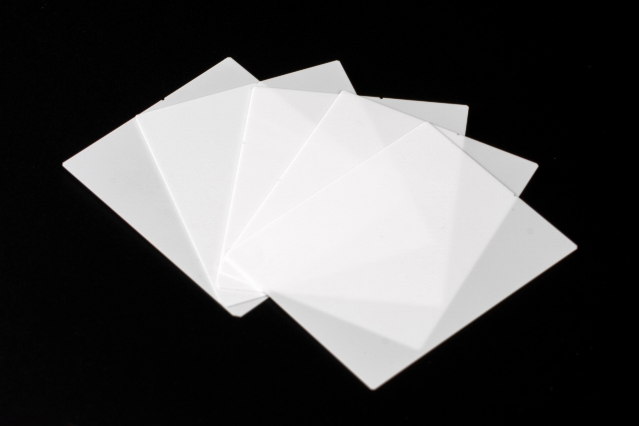
■ We perform dimensional measurement and rank classification using a high-resolution camera.
This can improve process yield, for example by reducing printing misalignment.
Slit classification is also available. For details, please see here.
■ Improvements to our pressing method have stabilized the breakability of the substrate, and the break edges are smooth.
■ The substrate has excellent surface smoothness and few voids (holes on the substrate surface), so it is also used for chip resistors in thin-film applications.
■ We can provide processing with minimal burrs.
■ Mold design, machining, and repair are all handled in-house.
[Main applications of Phonon Meiwa's Alumina 96% substrates]
- General thick film substrates
- Automotive component substrates
- Automotive thin film resistor substrates
- Sensor component substrates
- High-voltage resistor substrates
- Power module substrates
- Hybrid IC substrates